The Ovonic Cognitive Computer represents a breakthrough concept that is designed to fulfill the long-sought goal of achieving intelligent, machine-based computing. The concept relies on the creation of a densely interconnected network of “Ovonic Cognitive Devices” with functionalities based on the unique properties of chalcogenide materials. When so interconnected, Ovonic Cognitive Devices are designed to simulate the neurosynaptic behavior of biological neurons.
Like biological neurons, Ovonic Cognitive Devices are capable of receiving and weighting multiple inputs. They show threshold activation, i.e., an operational mode in which an Ovonic Cognitive Device accumulates input energy signals without responding until the total accumulated energy reaches a threshold level (critical crystalline volume fraction). Once the threshold (percolation limit) is reached, the Ovonic Cognitive Device undergoes an abrupt transformation from a high resistance state to a low resistance state in a process designed to mimic the firing of a biological neuron.
An individual Ovonic Cognitive Device is an Angstrom scale device that can be interconnected to many other Ovonic Cognitive Devices in two-dimensional arrays or in three dimensional, vertically integrated, networked arrays. The threshold level of individual Ovonic Cognitive Devices can be controlled by varying the thickness and chemical composition of the active chalcogenide material. As a result, neural-like arrays exhibiting rich functionality may be achievable.
The combination of small device size, intrinsic neurosynaptic device functionality and dense device interconnectivity in three dimensions using the Ovonic Cognitive Devices offers the potential for Ovonic Cognitive Computers to function with a highly parallel mode of operation that is designed to be reminiscent of the biological brain. Individual Ovonic Cognitive Devices within a network can also be configured to function as weighting devices that can be used to control the interconnection strength between Ovonic Cognitive Devices configured to function neurosynaptically. Since the interconnection strength is adjustable, networks formed from Ovonic Cognitive Devices are intended to display learning and adaptability properties analogous to those of biological neural networks. Finally, the active chalcogenide material used in the Ovonic Cognitive Devices and Ovonic Cognitive Computer is able to both process and store information and as a result, obviate the customary need to separate memory and CPU functions in computers.
To date, we have demonstrated addition, subtraction, multiplication, division, factoring, non-binary processing, modular arithmetic and encryption with Ovonic Cognitive Devices. The active chalcogenide material of the Ovonic Cognitive Devices and the Ovonic Cognitive Computer can be deposited in thin film fashion in a continuous manufacturing process using a proven technology.
In particular, the division algorithm that we have demonstrated can be easily expanded to perform factoring of large numbers and modular arithmetic through massively parallel operation. On this basis, it is possible that extremely fast search engines can be developed making use of the unprecedented parallelism and factoring of information instead of just numbers.
The scalability of the Ovonic Cognitive Devices and their proven compatibility with standard silicon manufacturing processes has the potential to allow billions of them to be interconnected in a dense network, offering a pathway to unique new capabilities.
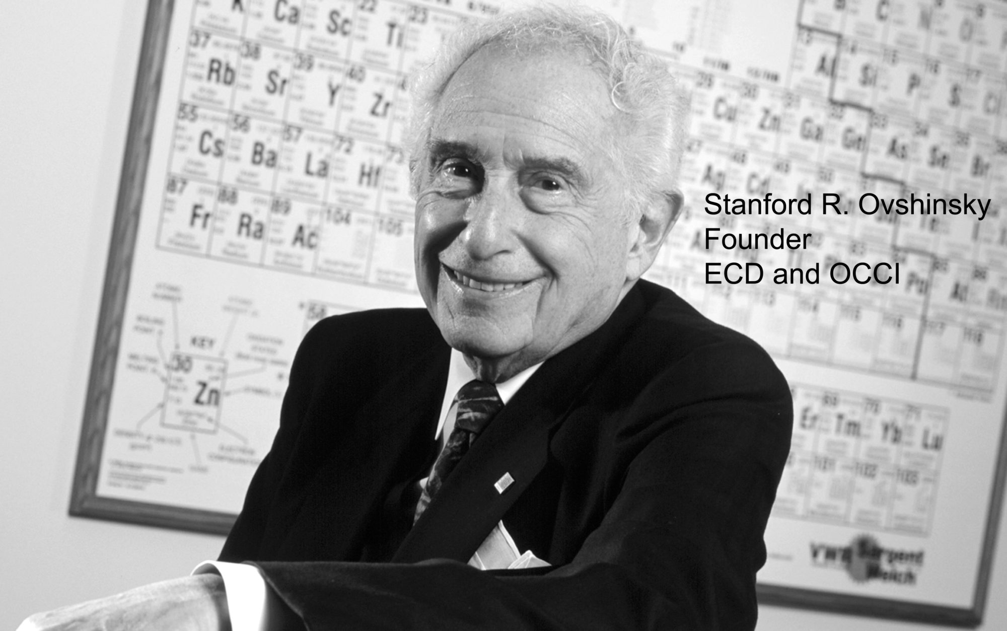
1955 – Stan Ovshinsky develops his ideas for cognition in a paper presented at Wayne State University Medical School entitled “Nerve Impulse”
1959 – Stan develops a switch using TaOx and a liquid electrolyte called the Ovitron
1961 – Stan begins developing a solid-state switch to perform similarly
1962 – Stan patents Metal Oxide RRAM devices
1963 – Exhaustive study of the switching properties of materials is undertaken
1964 – Chalcogenide alloys are employed, exhibiting both threshold and memory switching
1970 – Series connected threshold and memory switches make a radiation hard memory
1986 – Monolithic integration of threshold and memory switches make a 3D memory
1990 – Ge2Sb2Te5 is employed to make high performance memory
1996 – PCM scalability is demonstrated
1999 – Ovonyx is formed to commercialize PCM
2001 – Boil Pashmakov characterizes new ‘cognitive’ behavior in PCM
2002 – Ovonic Cognitive Computer, Inc. is formed to develop Cognitive Chalcogenide alloy Computers
2008 – Numonyx is formed and produces the first 4f2 3D nonvolatile memory array
2014 – Cognitive computer emulation becomes viable using TeraFLOP GPU computers
2015 – Intel/Micron announce 3D XPoint™, a high performance nonvolatile chalcogenide memory
2016 to Present – Ovonic Cognitive Computer continues their chalcogenide development work
2018 April 13 The Man Who Saw Tomorrow Stan Ovshinsky Biography available on Amazon.com
2019 July 7- “Stanford Ovshinsky and the Genisis of the Cognitive Computer”, Proc. IEEE, v.107 #7, pp1467-1463.
3D XPoint is a trademark of Intel Corporation in the U.S. and/or other countries